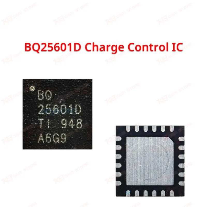
When a phone lands on your bench with a dead charging port, no fast charge, or a board that pulls current but never fills the battery, the charging IC is often the real culprit — and TI's BQ25601D sits at the center of many of these charging circuits. This chip works as a single-cell, I2C-controlled buck battery charger that handles both charging and power path duties on one die, so you're not chasing a failure across separate power FETs and a stand-alone charger controller.The BQ25601D pulls power from a 3.9V to 13.5V input range and delivers a battery charge voltage between 3.85V and 4.62V, covering the voltage window most Li-Ion and Li-Polymer phone batteries need. Its absolute maximum input rating sits at 20V, giving headroom against voltage spikes from a rough charger or a shorted cable — a common trigger for dead-after-charge boards you'll see on the bench. The chip switches at 1.5MHz in synchronous buck mode and hits 92% charge efficiency at 2A from a 5V input, so it runs cool enough for tight board layouts without extra heatsinking.Inside the package, TI integrates the reverse-blocking FET, high-side switching FET, low-side switching FET, and battery FET along with current sensing and loop compensation. Fewer discrete parts sit around the IC on the original board, which means fewer failure points for you to trace when a charging issue shows up. The chip also runs USB On-The-Go, delivering up to 1.2A on VBUS at 92% boost efficiency, which matters on devices that share one port between charging and OTG accessories.For fault-finding, the BQ25601D gives you real diagnostic hooks instead of guesswork. It auto-detects USB BC1.2, SDP, CDP, DCP, and non-standard adapters, so a "not fast charging" complaint often traces back to detection logic rather than a dead cell or a worn connector. The STAT and INT outputs report charging status and fault conditions directly, and the VBUS_GD bit tells you whether the board is even seeing a good power source — useful when you need to separate a charging IC fault from a bad charging port or a blown fuse. Thermal regulation kicks in at 110°C junction temperature and full thermal shutdown hits at 160°C, protecting the board from a cascading short on the charging rail.The IC runs in two modes — full autonomous operation with no software control needed, or I2C mode where a host processor adjusts charge current, input current limit, and voltage thresholds on the fly. On repair boards where you don't have access to original firmware, the device still initiates and completes a full charge cycle on its own: pre-conditioning, constant current, then constant voltage, with automatic termination and recharge threshold monitoring. That autonomous behavior lets you bench-test a replaced IC and confirm charging function even without full software access to the phone's charging stack.Battery leakage current sits at 17µA, low enough that phones sitting in shop inventory don't drain fast, and ±0.5% charge voltage accuracy keeps battery health stable across repeated charge cycles. NVDC power path management also lets a board power on and run with no battery installed or a deeply discharged cell — exactly the state you're often working with when a customer brings in a phone that's been dead for weeks.Package-wise, the BQ25601D ships in a 24-pin WQFN, 4mm x 4mm x 0.75mm — small enough to sit tight against other components on modern phone boards, so reballing and IC replacement calls for a fine-tip iron, proper flux, and a steady hand under the microscope. Match the exact IC marking against the original before swapping it in, since board designs built around this charging architecture vary by device and firmware calibration.If your workshop handles charging port repair, board-level charging circuit work, or IC replacement on phones with dead charging, no fast charge, or general charging issue complaints, the BQ25601D covers a wide slice of that workload with one part number.