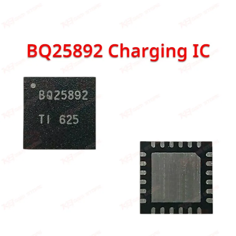
The BQ25892 sits at the center of a phone's power path. It is not a simple charger chip. It manages input detection, buck-mode charging, battery protection, system power delivery, and OTG boost output from a single WQFN-24 package. When a phone shows a dead-after-charge fault, a charging IC failure on this part number is one of the first components you check on many Android boards. This IC comes from Texas Instruments' bq2589x family and pairs a 5A switch-mode buck charger with an I2C serial interface for charging and system settings control. You get charge efficiency reaching 93% at 2A and 91% at 3A, which keeps thermal stress low on the board during fast charging. The wide input voltage limit range, 3.9V to 14V, lets the IC handle high-voltage adapters without external protection circuitry, and its Input Current Optimizer pulls maximum safe power from whatever adapter gets plugged in without overloading it. On your bench, this part explains a specific pattern: a phone that draws power and shows a charging icon but never actually charges, or one that gets warm near the charging port without current reaching the battery. Both point to the power path stage this IC controls. The BQ25892 also runs battery discharge through an 11-mΩ battery FET, so a board with abnormal battery drain or a phone that dies fast even on a "healthy" battery can trace back here too. The chip includes a 7-bit ADC that monitors VBUS, battery voltage, system voltage, and charge current in real time, and a PG (Power Good) output that flags whether a usable power source is present. If you're chasing an intermittent charging fault, that PG behavior often tells you whether the fault sits in the IC itself or further upstream at the charging port or filters. The device also runs thermal regulation, cutting charge current once junction temperature crosses 120°C, so a board that stops charging only after heavy use can indicate the IC is protecting itself rather than failing outright, worth checking before condemning the part. USB OTG support is built in too. The boost converter delivers an adjustable 4.5V to 5.5V output at up to 2.4A, which matters on boards where OTG file transfer or reverse charging has stopped working even though normal charging still functions. That symptom alone often isolates the fault to this IC rather than the connector or flex cable. Reballing this part calls for a proper WQFN-24 stencil and controlled reflow profile since the package uses a fine 0.5mm pitch with an exposed thermal pad. Preheat evenly, avoid excess flux pooling under the pad, and confirm continuity on VBUS, SYS, BAT, and the I2C lines (SCL/SDA) after mounting before you close the board back up. A cold joint on the thermal pad is a common cause of a "fixed for a day, dead again" comeback on this specific IC. KB GSM Store stocks the genuine BQ25892 for board-level replacement work, tested and ready for your reflow station. This is a precision part, so match the exact marking and pin orientation against the original chip before removal, since several related bq2589x variants share a similar footprint but differ in pinout details.