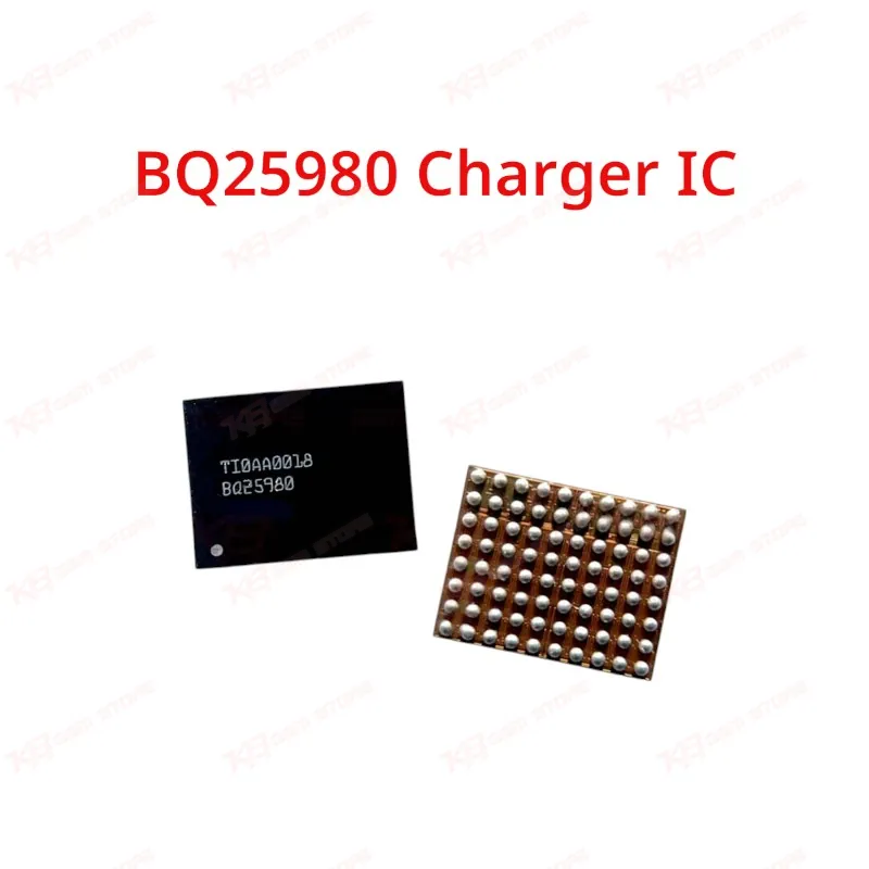
The BQ25980 sits at the core of high-wattage fast charging systems built around 2-cell (2S) battery packs. Texas Instruments designed this chip around a dual-phase switched capacitor topology, a method that pulls input current at roughly half the rate of the output charging current. On your repair bench, this matters because it explains why phones using this IC run noticeably cooler during fast charging and pull less current through the charging cable than older single-phase designs.I2C control gives the BQ25980 its flexibility. The chip talks to the phone's main SoC or a companion charger IC like the BQ25790, letting the system program charge voltage, current limits, and protection thresholds in real time rather than relying on fixed hardware values. When a phone comes in with a "charging but not fast charging" complaint, this is often where the fault traces back — a communication failure on this I2C line between the main charger and the BQ25980 stops fast charge negotiation even though basic slow charging still works.Input handling on this IC covers a wide range: it accepts 6V to 22V during normal operation, with support up to 40V when paired with an external ACFET, or 28V without one. Since battery charge voltage runs between 7.0V and 9.54V, exactly twice the single-cell voltage, the switched cap stage converts input voltage down at roughly a 2:1 ratio while doubling output current relative to input current, up to 4.75A per phase. This is the mechanism behind 65W-and-above fast charging on phones that use this chip.For technicians doing IC-level rework, the built-in 7A bypass mode is a practical feature to know. It routes current through internal MOSFETs with charging path resistance under 13mΩ, letting the phone fall back to a slower but still functional charging path when the older 10V adapter connects instead of a proper fast charger. If you're diagnosing a "charging slow after IC change" case, checking whether the phone dropped into bypass mode is a faster first step than assuming a bad reball.Protection coverage on the BQ25980 is dense for a chip this size. It carries input overvoltage and battery overvoltage protection, input and battery overcurrent protection, output overvoltage protection, input undercurrent and reverse-current detection to catch adapter unplug events, input short-circuit protection, temperature monitoring on both the battery and the connector, and junction overtemperature shutdown. A 16-bit ADC continuously reads bus voltage, bus current, output voltage, battery voltage, battery current, connector temperature, battery temperature, and die temperature — data the phone's software layer uses to manage the whole charging cycle. When this ADC reports bad values after a reflow, expect erratic charging behavior or a charging icon that won't hold steady.The IC also includes a dual-input power mux controller with driver support for external N-FET switching, allowing designs with two physical input paths, useful in phones that support both wired fast charging and reverse wireless charging through a shared power rail. Two synchronized BQ25980 units can run in parallel for combined charging current up to 12A, a configuration found in some higher-wattage flagship boards.Packaged in an 80-pin DSBGA measuring roughly 4.071mm by 3.195mm, the BQ25980 demands hot air precision and a steady hand during removal and reballing. Board temperature control and correct stencil alignment matter more here than on larger QFN parts, since pad pitch on this package leaves little margin for misalignment.