


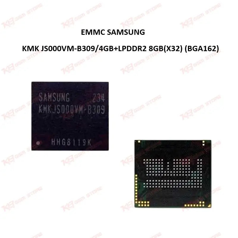
EMMC SAMSUNG KMKJS000VM-B309/4GB+LPDDR2 8Gb(x32) (BGA162)
EMMC SAMSUNG KMKJS000VM-B309/4GB+LPDDR2 8Gb(x32) (BGA162)
Regular price
Rs.800.00 PKR
Regular price
Sale price
Rs.800.00 PKR
Shipping calculated at checkout.
Quantity
Couldn't load pickup availability
The Samsung KMKJS000VM-B309 is a multi-chip package (MCP) combining 4GB eMMC NAND flash storage with 8Gb (x32) LPDDR2 mobile DRAM in a single BGA162 footprint. This IC handles both storage and system memory duties on the board, making it a core replacement part for dead-after-flash boards, boot loop cases, and hang-on-logo faults where the eMMC or RAM side has failed. Built on Samsung's original MCP architecture, it is the correct choice when board-level diagnosis points to a bad combo memory chip rather than a software fault. Suited for technicians doing IC reballing and jumper-level board repair on Android devices using this exact chip footprint.
⚖️ Weight: 0.01 kg
SKU:MST-IC-4
- Safe & Secure Payment
- Fast Delivery
- WhatsApp Support


Description
FAQ
What is the product name?
The product name is Samsung KMKJS000VM-B309 eMMC 4GB + LPDDR2 8Gb (x32) BGA162 MCP IC.
What is the brand of this product?
The brand of this product is Samsung.
What is the model of this product?
The model of this product is KMKJS000VM-B309.
What is this product used for?
This product is used for board-level replacement of failed combo eMMC and LPDDR2 memory chips in Android phones.
Which devices are compatible with this product?
This product is compatible with Android boards designed around the BGA162 combo memory footprint matching this chip's pinout.
Who should use this product?
This product is suitable for mobile repair technicians, repair shops, service centers, and professional users.
Does this chip need to be reballed before installation?
Yes, the KMKJS000VM-B309 comes in a bare BGA162 package and requires reballing with a stencil matched to this ball count before reflow onto the board.
Will the phone boot without reflashing after swapping this chip?
If the replacement chip carries firmware from a confirmed-good donor board, the phone typically boots without a fresh flash, though a blank chip will require programming through your box or programmer first.