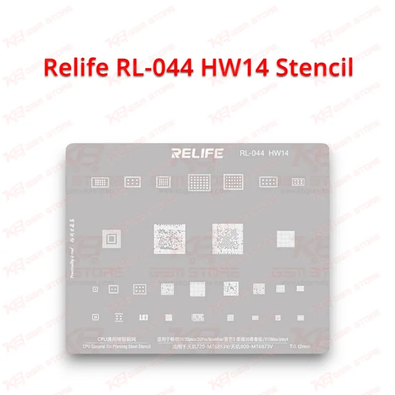
Board-level repair work on Huawei-family devices demands a stencil that lines up with BGA pads the first time, and the Relife RL-044 HW14 Stencil is built around that exact requirement. Build and Material — the stencil is cut from ultra-thin, high-quality stainless steel that resists thermal deformation even after repeated hot air cycles, so a technician running the same layout dozens of times a week doesn't watch it warp or bow out of shape. Hole Geometry — the round-square hole pattern common to the RL-044 family is engineered to let solder paste release cleanly off the mesh, which keeps ball height uniform across the pad grid instead of leaving thin spots that cause a dead-after-flash outcome on reassembly. Half-Etched Protection — sections of the steel around sensitive zones are half-etched rather than fully cut, forming shallow grooves that let neighboring components sit flush against the board during reflow, shielding them from direct heat while the target IC is being reballed. Cooling Design — small ventilation cutouts worked into the stencil body help heat dissipate faster during hot air work, reducing the risk of scorching the PCB laminate or lifting nearby pads when working close to power management ICs. In a typical repair shop workflow, the RL-044 HW14 layout comes into play after a chip has already been removed for testing or replacement: the technician cleans the pad, aligns the RL-044 HW14 stencil over the footprint, applies solder paste or drops solder balls through the mesh, then reflows with a hot air station before lifting the stencil away. This is the same sequence used for board cleaning after liquid damage, for charging IC replacement after a persistent charging issue, and for power IC reballing when a board shows a hardware fault instead of a software fault. Because the stencil is a passive tooling accessory rather than a powered device, there's no calibration or firmware step involved — its value comes entirely from how precisely the holes match the target pad layout, which is why Relife lasers each stencil rather than stamping it. For a Pakistani repair bench juggling mixed brands in one day, having a dedicated HW14 layout on hand means not having to improvise with a universal stencil that only approximates the pad spacing, which is often where solder bridges and hang on logo symptoms after a repair actually come from. The stencil pairs naturally with a reballing kit for BGA balls, a non-magnetic spatula for paste spreading, and a PCB holder to keep the board steady during alignment, and it fits into the same upgrade path as ISP pinout tools and eMMC programmers for shops building out a full board-repair station rather than just a flashing bench. Storage matters too — keeping the RL-044 HW14 stencil flat between uses, away from bending stress, preserves hole accuracy far longer than tossing it loose into a tool drawer, since even minor warping throws off pad alignment on the next job.