


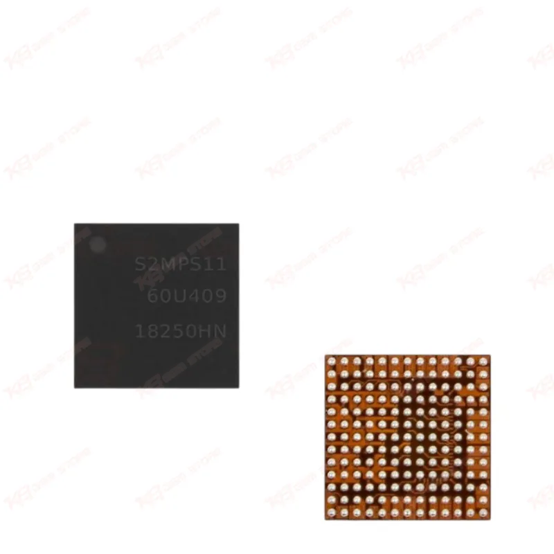
S2MPS11 Power IC
S2MPS11 Power IC
Regular price
Rs.350.00 PKR
Regular price
Sale price
Rs.350.00 PKR
Shipping calculated at checkout.
Quantity
Couldn't load pickup availability
The S2MPS11 is the main power management IC used on Samsung Galaxy S4 (GT-I9500) and Galaxy Note 3 (SM-N900 / SM-N9005) motherboards. It handles battery charging regulation and distributes stable power across the board's buck converter and LDO rails. When this IC fails, technicians usually see a dead phone, no charging response, or random shutdown on logo. This is a genuine BGA replacement chip for board-level repair, meant for technicians who reball and reflow rather than swap connectors. Requires a hot air station and proper BGA rework skill to install correctly.
⚖️ Weight: 0.01 kg
SKU:MST-IC-67
- Safe & Secure Payment
- Fast Delivery
- WhatsApp Support


Description
FAQ
What is the product name?
The product name is the Samsung S2MPS11 Power Management IC.
What is the brand of this product?
The brand of this product is Samsung Semiconductor.
What is the model of this product?
The model is S2MPS11, with the S2MPS11B2 variant used on Note 3 N900 boards.
What is this product used for?
This IC manages battery charging regulation and distributes power across the motherboard's buck converter and LDO rails.
Which devices are compatible with this product?
This IC is compatible with the Samsung Galaxy S4 (GT-I9500) and Galaxy Note 3 (SM-N900 / SM-N9005).
Who should use this product?
This product is suitable for mobile repair technicians, repair shops, service centers, and professional BGA rework technicians.
Does replacing this IC fix a dead phone or no-charging fault?
Yes, when the fault traces to a failed power or charging rail on this IC rather than the battery, port, or a separate board short.
Can this IC be hand-soldered, or does it need BGA rework tools?
It requires BGA rework — a hot air station and proper reballing setup, since it mounts via solder balls with no leads for manual soldering.