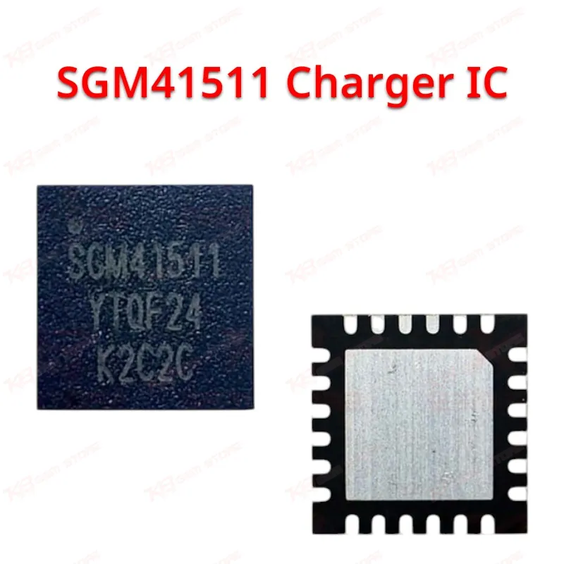
Charging failures remain one of the most common board-level faults you handle on the repair bench, and the SGM41511 sits at the center of that workflow in a wide range of smartphones and portable systems. This IC is a battery charger and system power path management device that combines a synchronous buck converter with four integrated power switches: an input reverse blocking FET (RBFET), a high-side switching FET, a low-side switching FET, and a battery FET that manages the connection between the system rail and the battery. That level of integration means fewer discrete components on the board and a tighter, more efficient power path, which also means a single IC failure can take down charging entirely.The SGM41511 accepts a 3.9V to 13.5V operating input, with a sustainable voltage rating up to 20V, so it tolerates the voltage spikes and inconsistent adapters technicians see on real devices in the field. Switching at 1.5MHz through its synchronous buck stage, it reaches up to 93% charge efficiency at 1A and 91% at 2A when running from a standard 5V USB input, keeping heat generation low during fast charging cycles. The charger supports charge currents up to 3A, matching the demands of modern single-cell Li-Ion and Li-Polymer battery packs used in current-generation smartphones and tablets.I2C programming is what separates this chip from simpler autonomous chargers. Through the I2C bus, host processors can adjust charge current, input current limits, and voltage thresholds on the fly, which is exactly why you find this class of IC in devices with adaptive fast-charging profiles. When no host command is present, the SGM41511 still operates like an autonomous charger, running a default 6-hour fast charging safety timer and progressing through pre-conditioning, constant current, and constant voltage phases based on sensed battery voltage. This dual behavior — smart when controlled, safe when standalone — is useful context when you're diagnosing a board where the host processor itself may be faulty.For OTG use cases, the SGM41511 can reverse power flow and supply 5V at up to 1.2A out through VBUS, a detail worth checking when a device shows OTG/reverse-charging faults rather than a straightforward charging issue. The TS pin connects to an NTC thermistor for battery temperature monitoring, and the IC follows JEITA-based charge profiles, suspending or limiting charge current when the battery reports temperatures outside safe cool or warm windows. Combined with over-voltage protection, over-current protection, input UVLO, and thermal shutdown, this gives the charging circuit multiple protection layers — useful to know when tracing why a board refuses to charge even though the adapter and cable test fine.Physically, the SGM41511 ships in a QFN-24 package, a compact leadless format that demands a hot air rework station with tight temperature control and a fine nozzle for clean removal and reballing. Board-level symptoms tied to this IC typically include no charging, charging shown but current not rising, charging IC running hot, dead after liquid damage near the charging circuit, or intermittent charging tied to a cracked solder joint under the package. Because the RBFET and BATFET sit inside this single IC, a short or open fault here can also present as a completely dead board with no power path to the system rail at all — a pattern GSM technicians should rule this IC into or out of early in the diagnostic sequence.As a system power path IC rather than a simple linear charger, the SGM41511 fits into the broader charging and power management workflow alongside PMICs, protection ICs, and battery fuel gauge chips on the same board, so a full charging-circuit repair often means checking these related components together rather than replacing this IC in isolation.