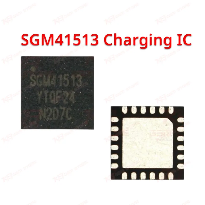
Charging issue complaints are one of the most common jobs on any mobile repair bench, and a large share of them trace back to the charger IC rather than the charging port itself. The SGM41513 is exactly this type of component — a single-cell battery charger and system power path management IC from SGMICRO, designed to sit between the USB input and the battery, controlling how power flows into the phone and how the battery charges. At its core, the SGM41513 integrates four power switches: an input reverse-blocking FET, a high-side switching FET, a low-side switching FET, and a battery FET. This full integration means you get charging, power path switching, and battery FET control from a single chip, instead of chasing separate discrete components across the board. For a technician doing board-level diagnostics, this matters — a dead phone with no charging response often narrows down to this one IC once the port and battery connector test clean on the multimeter. The chip runs a synchronous buck charger at 1.5MHz switching frequency, accepting an input voltage range of 3.9V to 13.5V while sustaining up to 22V without damage. That headroom is useful when a board has been exposed to a bad charger or voltage spike — the IC is built to tolerate short-term overvoltage without failing outright, though sustained high voltage exposure can still degrade or kill the part. Charge current output reaches up to 3A, with efficiency rated at 93.8% at 1.02A from a 5V input and 89.8% at 2A from a 9V input, so the IC is tuned for both standard USB and higher-voltage fast-charge adaptors. I2C programming is where this IC becomes flexible rather than fixed-function. Charge current, input current limit (IINDPM), and input voltage limit (VINDPM) can all be set through the I2C interface, and Dynamic Power Management automatically pulls back charge current if the input source can't sustain the load. This is the same behavior you'll recognize from phones that "trickle charge" under a weak adaptor instead of cutting off — the SGM41513 is managing that transition internally rather than leaving it to firmware alone. On the OTG side, the IC boosts battery voltage to supply 5.15V on VBUS with up to 1.2A output, which covers reverse charging or accessory-powering scenarios on devices that support it. Safety protections built into the chip include input UVLO, input overvoltage (ACOV) protection, thermal regulation, thermal shutdown, and NTC-based battery temperature monitoring through the TS pin — all of which reduce the chance of a repeat failure if the root cause was a heat or voltage-related fault rather than a workshop ESD event. For board-level work, this IC ships in a TQFN-4×4-24L package — a small leadless footprint that demands a hot air station with fine nozzle control and steady temperature profile, along with flux and paste suited to fine-pitch QFN work. Because the package is leadless, alignment under the microscope before reflow is critical; a shifted IC on reflow is one of the more common causes of a board that still won't charge after a first replacement attempt. Typical symptoms that point to this IC include: phone not charging despite a good port and cable, charging LED not turning on, charging that starts and stops intermittently, or a board that draws no current at all when connected to a bench power supply. Before swapping the IC, technicians should confirm continuity on VBUS and PMID lines and rule out a shorted battery FET or blown TVS diode nearby, since power path faults on the same rail can mimic a dead charger IC.