


Brand:
YCS
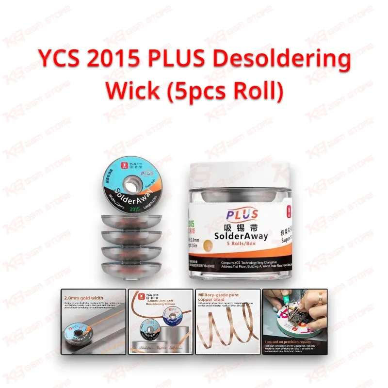
YCS 2015 PLUS Desoldering Wick (5pcs Roll)
YCS 2015 PLUS Desoldering Wick (5pcs Roll)
Regular price
Rs.1,350.00 PKR
Regular price
Sale price
Rs.1,350.00 PKR
Shipping calculated at checkout.
Quantity
Couldn't load pickup availability
The YCS 2015 PLUS Desoldering Wick (5pcs Roll) gives you five rolls of 2.0mm braided pure copper wick, each roughly 1.5m long, for fast and clean solder removal on mobile motherboards. The rosin-treated braid pulls molten solder off IC pads, BGA pads, and charging connector pins with less heat and fewer passes, so you protect nearby components while you prep the board. Use it after you lift a PMIC or CPU, before reballing, or whenever you need to clear a solder bridge. The 5-roll pack keeps your repair bench stocked for daily board-level work at a solid price in Pakistan.
SKU:MST-SOLDERING-ACCESSORIES-680
⚖️ Weight: 0.01 kg
- Safe & Secure Payment
- Fast Delivery
- WhatsApp Support


Description
FAQ
What is the product name?
The product name is YCS 2015 PLUS Desoldering Wick (5pcs Roll).
What is the brand of this product?
The brand of this product is YCS.
What is the model of this product?
The model of this product is 2015 PLUS.
What is this product used for?
This product is used for removing solder from PCB pads, IC footprints, BGA areas, and connector pins during mobile phone repair.
Which devices are compatible with this product?
This product is compatible with all mobile phone motherboards and electronic PCBs, as it works universally and is not device-specific.
Who should use this product?
This product is suitable for mobile repair technicians, repair shops, service centers, and professional users.
Can the YCS 2015 PLUS Desoldering Wick remove lead-free solder from mobile boards?
Yes. Lead-free solder melts at a higher temperature, so raise your iron temperature slightly and add fresh flux to the pads before you drag the wick for a clean pickup.
Is a 2.0mm wick width right for cleaning CPU BGA pads?
Yes. The 2.0mm width covers mobile CPU and eMMC BGA pad fields with controlled heat; for large ground planes or wide shield areas, a 3.5mm wick works faster.