


Brand:
YCS
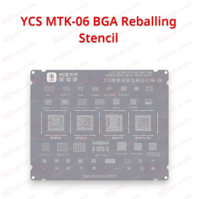
YCS MTK-06 BGA Reballing Stencil
YCS MTK-06 BGA Reballing Stencil
Regular price
Rs.600.00 PKR
Regular price
Sale price
Rs.600.00 PKR
Shipping calculated at checkout.
Quantity
Couldn't load pickup availability
YCS MTK-06 Stencil for MediaTek Chip Reballing
The YCS MTK-06 BGA Reballing Stencil gives your repair bench a dedicated template for rebuilding solder balls on MediaTek (MTK) chips after removal. When a dead phone, hang on logo fault, or network issue traces back to a cracked BGA joint, you lift the chip, clean the pads, and use this stencil to lay a fresh, even ball grid. A dedicated MTK pattern saves you the time you would spend hunting for a matching footprint on a crowded universal plate. Pair it with solder paste, flux, and a hot air station, and you get a repeatable reballing routine for daily MTK board-level work in your shop.
SKU:MST-SOLDERING-TOOLS-976
⚖️ Weight: 0.01 kg
- Safe & Secure Payment
- Fast Delivery
- WhatsApp Support


Description
FAQ
What is the product name?
The product name is YCS MTK-06 BGA Reballing Stencil.
What is the brand of this product?
The brand of this product is YCS.
What is the model of this product?
The model of this product is MTK-06.
What is this product used for?
This product is used for reballing MediaTek (MTK) chips during board-level mobile phone repair.
Which devices are compatible with this product?
This product is compatible with the MediaTek (MTK) chip models marked on the stencil and the phones that use those chips.
Who should use this product?
This product is suitable for mobile repair technicians, repair shops, service centers, and professional users.
How do I confirm the YCS MTK-06 stencil matches my MTK chip?
Read the part number printed on your IC and compare it with the chip markings on the stencil. Then place the chip under the stencil and check under a microscope that every opening sits centered over a pad before you apply paste.
Why do solder balls bridge or come out uneven when I reball an MTK chip?
Uneven or bridged balls usually come from dirty pads, too much paste in the openings, or a stencil that lifts during heating. Clean the pads with IPA, scrape excess paste off with a blade, hold the stencil flat at the edges, and keep the hot air moving instead of heating one spot.