


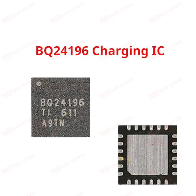
BQ24196 Charging IC for Enhanced Device Charging
BQ24196 Charging IC for Enhanced Device Charging
Regular price
Rs.180.00 PKR
Regular price
Sale price
Rs.180.00 PKR
Shipping calculated at checkout.
Quantity
Couldn't load pickup availability
The BQ24196 is a genuine Texas Instruments single-cell Li-Ion/Li-Polymer switch-mode battery charger IC used across smartphones and tablets with I2C-controlled charging architecture. It delivers up to 2.5A charge current with Narrow VDC power path management, letting the connected device stay powered even on a dead or deeply discharged battery. Built for GSM repair benches handling charging faults, dead-after-flash boards, and no-charging complaints, this IC replaces damaged charging PMICs on boards where the original chip has failed due to short circuit, moisture damage, or reverse voltage. Suitable for professional reballing and IC change work.
⚖️ Weight: 0.01 kg
SKU:MST-IC-114
- Safe & Secure Payment
- Fast Delivery
- WhatsApp Support


Description
FAQ
What is the product name?
The product name is the BQ24196 Charging IC.
What is the brand of this product?
The brand of this product is Texas Instruments.
What is the model of this product?
The model of this product is BQ24196 (BQ24196RGER package variant).
What is this product used for?
This product is used for board-level replacement of the charging PMIC on phones and tablets with no-charging, slow-charging, or dead-after-flash charging faults.
Which devices are compatible with this product?
This product is compatible with smartphones and tablets built around single-cell Li-Ion/Li-Polymer switch-mode charging architecture that originally use the BQ24196 as their charging IC.
Who should use this product?
This product is suitable for mobile repair technicians, hardware engineers, repair shops, and service centers performing board-level charging IC repair.
Does the BQ24196 support USB OTG output?
Yes, it includes a built-in synchronous boost converter that outputs 5V at 1.3A for USB OTG operation.
What input current limit settings does the BQ24196 support?
It supports eight input current limit steps: 100mA, 150mA, 500mA, 900mA, 1.2A, 1.5A, 2A, and 3A, selectable through I2C or default hardware settings.