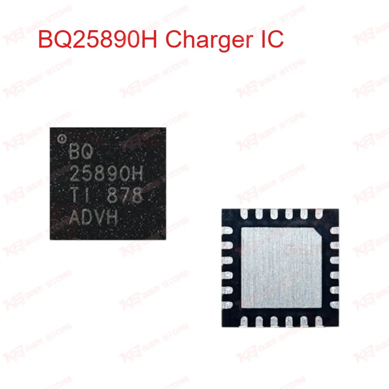
The BQ25890H handles two jobs on a phone mainboard that used to need separate chips: it charges the battery and it manages system power path at the same time. You get a single I2C-controlled IC doing 5A switch-mode buck charging while also routing power between the input source, the system rail, and the battery — all in a compact 24-pin WQFN package measuring just 4mm x 4mm x 0.75mm. On your repair bench, this chip shows up most often on boards with a "dead after flash" symptom, a phone that shows charging animation but never gains percentage, or a board that draws current but never boots past logo. Since the BQ25890H sits directly in the power path between VBUS, the battery, and the system rail, a damaged unit often mimics a dead motherboard fault even when the CPU and PMIC are healthy. Testing continuity on the input and output pins with a multimeter before condemning other ICs saves you from unnecessary rework. Input handling on this IC covers 3.9V to 14V, with an absolute maximum rating of 22V, so it survives most adapter-related overvoltage events that kill weaker charger ICs outright. Input current limit adjusts from 100mA to 3.25A in 50mA steps, letting the chip auto-detect USB SDP, CDP, DCP, and non-standard adapters without host intervention. This auto-detection matters on repair jobs where the original firmware calibration is uncertain — the IC still negotiates a safe charging current on its own. The Input Current Optimizer (ICO) function pulls maximum available power from whatever adapter is connected without tripping its overload protection, which is why phones repaired with this IC often charge faster than expected on generic Pakistani market adapters that don't declare exact wattage. Resistance Compensation (IRCOMP) compensates for voltage drop across PCB traces and connectors, useful on boards where the charging port or flex cable has slightly degraded contact resistance from repeated use. Charge efficiency reaches 93% at 2A and 91% at 3A output, both measured at the IC's rated 1.5MHz switching frequency. Regulation accuracy stays tight: ±0.5% on charge voltage, ±5% on charge current, and ±7.5% on input current — figures that matter when a technician is trying to diagnose whether a "charging issue" complaint traces back to the IC itself or to a downstream battery or connector fault. Battery discharge runs through an integrated 11mΩ BATFET rated up to 9A, supporting Narrow VDC (NVDC) power path management. This means the system can power on and operate even with no battery installed or with a deeply discharged battery — a feature directly useful when testing a board after IC change karna, since you can verify system boot before reconnecting the original battery. USB OTG boost mode outputs an adjustable 4.5V to 5.5V with up to 2.4A current, switchable between 500KHz and 1.5MHz operation. On devices where OTG function stopped working after a liquid damage or drop event, this IC is one of the first suspects, since the boost converter shares silicon with the buck charger path. Safety protections built into the chip include battery temperature thermistor monitoring under both JEITA and hot/cold profiles, thermal regulation that reduces charge current once junction temperature crosses 120°C, and full overvoltage/overcurrent protection on both input and battery paths. A STAT pin reports charging status directly, and an INT pin notifies the host system immediately when a fault condition triggers — both useful test points when diagnosing a board without full firmware access. For technicians running an ISP box or working through eMMC/UFS-related board faults, keep in mind the BQ25890H is strictly a power management IC and plays no role in flashing, software marna, or FRP/pattern operations. Its function stays confined to charging and power path — pairing it correctly with board schematics prevents wasted diagnostic time on unrelated software issues.