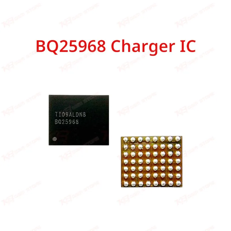
The BQ25968 works as the secondary fast-charge stage in a dual-charger system, sitting alongside a primary charger IC like the BQ25890 or BQ25896 on the same board. Instead of a standard buck converter, TI built this chip on switched-capacitor architecture — a 2:1 charge-pump design that pushes charging efficiency up to 97% while keeping the cable current at roughly half of what actually reaches the battery. That cuts heating in the charging cable and connector, which matters when you are troubleshooting a phone that gets hot during fast charge or shuts off charging mid-session.On the input side, the BQ25968 accepts 3.2V to 12V with a 20V absolute maximum rating, so it survives voltage spikes from aftermarket adapters without instantly failing — though repeated overvoltage exposure still degrades the die over time, which you will see as intermittent charging faults before a hard dead-IC failure. Battery-side, it regulates charge voltage between 3.5V and 4.65V, covering standard single-cell Li-Ion and Li-Polymer packs as well as LiFePO4 chemistry. Maximum charge current tops out at 6A, which is why you find this IC specifically on phones marketed with 33W, 65W, or higher fast-charge ratings rather than budget models running basic 10W charging.Communication with the host runs over I2C, so the primary charger and system PMIC negotiate charging state through firmware rather than fixed hardware thresholds. That is exactly why a bad BQ25968 often shows up as a software-visible fault: the phone reports "not charging" or drops to slow trickle charging even though the port itself tests fine and the battery holds charge normally once removed and tested externally. Built-in BAT temp thermistor monitoring with hot/cold profile support and IC thermal regulation add another layer — if you are chasing a board that charges fine cold but cuts off once it warms up, this thermal protection circuit inside the chip is worth checking before you condemn the battery or connector.For diagnosis on the bench, treat the BQ25968 as a likely suspect whenever a Xiaomi, Redmi, or POCO board shows charging issue symptoms after a phone gets wet, drops, or comes in dead after flash with the primary charger IC already confirmed good. Test continuity and resistance to ground on the VBUS and SW pins first — a shorted switched-cap IC is a common cause of a board pulling excess current and killing the charger port or even the PMIC downstream. Reflow first if you suspect a cold joint or hairline crack from board flex; if reflow does not restore charging detect, move to IC change. Use hot air with a proper stencil for the DSBGA-56 footprint, since this package uses a fine ball-grid array that does not tolerate rough reballing or misaligned placement.Because the chip talks over I2C and interacts directly with the primary charger's negotiation logic, always confirm firmware and EDL box compatibility before assuming a hardware fault — some charging-not-detect symptoms trace back to a corrupted charging profile in software rather than the IC itself, so box chalana and reading out charging parameters is a reasonable first step before jumper lagana or IC change. Keep antistatic precautions in mind throughout, since ESD damage to this chip is a common cause of premature failure even on boards with no visible physical damage.