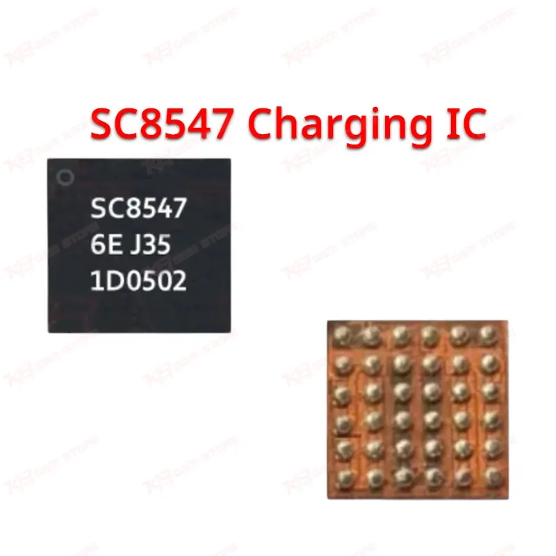
When a phone stops fast charging or shows a charging issue despite a healthy battery and connector, the switched capacitor charge pump is often the real fault point, and the SC8547 sits exactly at that stage of the power path. This chip is SOUTHCHIP's 6A switched capacitor direct charger, built around a 2:1 charge pump topology rather than a traditional linear or inductive converter. That distinction matters on your repair bench: a 2:1 charge pump moves current from input to battery at roughly half the input current relative to the output current, which is why cable and connector currents stay lower even during high-wattage fast charging. The architecture behind the SC8547 uses integrated FETs optimized for a 50% duty cycle. In practical terms, the current pulled through the charging cable is about half of what actually reaches the battery. This reduces resistive losses along the charging path and limits the temperature rise you would otherwise see during sustained fast-charge sessions. For technicians dealing with a phone that gets hot while charging or shuts off charging after a few minutes, this is often the exact behavior the original SC8547 was designed to prevent, and it is also what fails first when the chip itself degrades. Electrically, the SC8547 accepts an input voltage range of 3V to 11V, with an absolute maximum input rating of 20V, and regulates an output voltage range of 3V to 5V suited to single-cell battery charging in smartphones and tablets. Maximum output current is rated at 6A, which aligns with the higher-wattage fast-charge standards used in current-generation Android devices. The chip does not support a bypass mode, so it operates strictly in switched capacitor conversion during active charging cycles. Two integrated features extend the SC8547's role beyond simple power conversion. It includes an integrated ADC, which lets the host charging management system monitor voltage and current parameters directly through the chip rather than relying on external sensing circuitry. It also integrates VOOC PHY support, tying it into OPPO's VOOC fast-charging protocol stack alongside compatible charge-pump-based fast-charge implementations used across several Android OEMs. This combination is why the SC8547 shows up specifically in devices built around switched-capacitor fast-charge architectures rather than older buck-converter charging designs. Physically, the SC8547 is packaged in a CSP36 chip-scale package, which means precise reflow control and a clean board pad are essential during replacement. Because it sits directly in the charging current path, a failed SC8547 typically presents as no fast charging, charging that drops to a slow trickle, charging that cuts out under load, or a phone that draws power but never registers a charge percentage increase. In more severe failure cases tied to ESD or liquid damage, you may see a completely dead charging response even though the connector and battery test fine independently. On the repair bench, replacing the SC8547 is a board-level micro-soldering job. After confirming the fault sits at the charge pump stage through voltage tracing rather than the connector, PMIC, or battery, technicians desolder the failed CSP36 package, clean the pads, and reball or hand-solder the replacement using the correct reflow profile for CSP packages. Getting orientation and thermal profile right on the first attempt matters here, since CSP36 pads are dense and repeated reflow cycles risk pad lifting. Because the SC8547 is used across multiple device platforms sharing the same SOUTHCHIP charge-pump charging architecture, stocking genuine units gives you a reliable fix for a specific and recurring fault category rather than a guess-and-check replacement.