


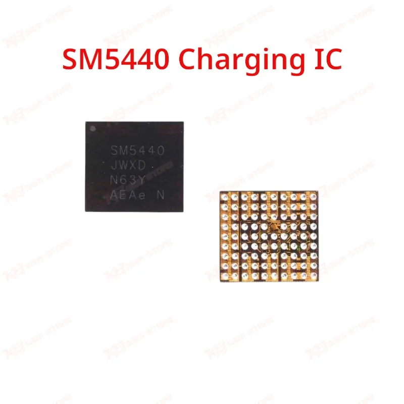
SM5440 Charging IC
SM5440 Charging IC
Regular price
Rs.350.00 PKR
Regular price
Sale price
Rs.350.00 PKR
Shipping calculated at checkout.
Quantity
Couldn't load pickup availability
The SM5440 is a Silicon Mitus switched capacitor charging IC built for fast, high-efficiency power delivery in Samsung smartphones. Rated up to 9A charging current with efficiency reaching 98%, it handles the charging path, input current limiting, and battery voltage regulation on the motherboard. On your repair bench, this is the chip you reach for when a Samsung device shows dead phone, not-charging, or charging IC fault symptoms. Programmable through I2C, it carries a 13-bit ADC for real-time voltage and current monitoring. A reliable pick for board-level charging repairs on S10 Plus, S6, S7, S8, J7, M30, A20s, and Fold boards.
⚖️ Weight: 0.01 kg
SKU:MST-IC-258
- Safe & Secure Payment
- Fast Delivery
- WhatsApp Support


Description
FAQ
What is the product name?
The product name is SM5440 Charging IC.
What is the brand of this product?
The brand of this product is Silicon Mitus.
What is the model of this product?
The model is SM5440.
What is this product used for?
This IC controls the charging path and battery voltage regulation on the motherboard, and it's used to repair dead phone and not-charging faults.
Which devices are compatible with this product?
This IC is compatible with Samsung Galaxy S10 Plus, Fold, A20s, J7, M30, S6, S7, S8, and C900.
Who should use this product?
This product is suitable for mobile repair technicians, repair shops, service centers, and professional users.
What is the maximum charging current the SM5440 supports?
The SM5440 supports switched capacitor charging up to 9A maximum, based on the input current limit configured through I2C.
Does the SM5440 support software configuration through I2C?
Yes, it runs on a 400kHz full-speed I2C interface that programs input current limit, VBAT regulation, thermal thresholds, and OVP settings.