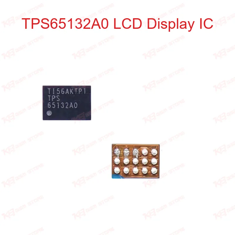
Every TFT-LCD panel needs a stable positive and negative voltage rail to drive its source driver IC correctly, and the TPS65132A0 exists to generate exactly that. This Texas Instruments power IC belongs to the TPS65132 family, a single-inductor dual-output (SIDO) converter series designed specifically for LCD bias applications in mobile devices. Instead of using two separate inductors to create a positive rail and a negative rail, the TPS65132A0 uses a shared inductor architecture, which keeps the PCB footprint tight and matches what you find on compact smartphone and tablet boards. On your repair bench, this IC sits between the battery/system rail and the display connector's bias lines. It accepts an input voltage range of 2.5V to 5.5V and steps it up to a fixed VPOS output of +5.0V while simultaneously inverting a portion of that energy down to a VNEG output of -5.0V. The A0 variant is factory pre-programmed with these exact voltage levels, so it ships ready to drive standard TFT-LCD bias requirements without extra firmware configuration on most boards. Maximum output current sits at 80mA on the VPOS rail and 40mA on VNEG, enough headroom for panels up to roughly 10 inches, covering the SFF to MFF (small form factor to mid form factor) range that includes phones and small tablets. Control runs over an I2C bus, giving the host processor the ability to manage power-up and power-down sequencing, enable or disable each rail independently through the ENP/ENN pins, and program active output discharge behavior. This matters on the repair side because a misbehaving sequencing setup, corrupted register state, or a shorted output line often shows up as "hang on logo," flickering display, or a completely dead panel even when the rest of the board tests fine. The chip also carries greater than 1000x programmable non-volatile memory, undervoltage lockout, and thermal protection, so a genuine component failure usually points to a hard short on VPOS/VNEG, a damaged inductor, or ESD damage on the input pin rather than a software-only fault. Efficiency stays above 85% at output currents over 10mA and climbs past 90% above 40mA, which keeps thermal stress low even on a densely packed board. Output voltage accuracy holds at 1% across the full operating temperature range, a spec that matters when you're chasing intermittent display issues that only appear under load or heat. The TPS65132A0 ships in a 15-ball DSBGA (chip-scale) package measuring 1.4mm x 2.2mm, which means reballing or replacing this IC demands a hot air rework station with tight temperature control, fine-tip tweezers, and a stencil matched to the exact ball pitch. Standard symptoms that point to this IC on your workbench include a phone that powers on and boots normally (confirming the main PMIC and CPU are alive) but shows a blank, white, or black display, or a panel with backlight but no image — a classic sign that VPOS/VNEG bias is missing while the rest of the display driver chain still receives power. Before condemning the IC, check the inductor and bias-rail capacitors for shorts, verify the input rail with a multimeter, and confirm the I2C lines aren't shorted to ground, since board-level shorts on VPOS or VNEG will often blow the IC repeatedly even after a successful reballing job. For technicians running an ISP or board-level repair workflow, the TPS65132A0 is a common line item alongside other display bias and PMIC-family parts, and it pairs naturally with a decent hot air station, a fine-pitch stencil kit, and a reliable multimeter for pre- and post-repair voltage checks.